NRL designs multi-junction solar cell to break efficiency barrier
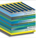
U.S. Naval Research Laboratory scientists in the Electronics Technology and Science Division, in collaboration with the Imperial College London and MicroLink Devices, Inc., Niles, Ill., have proposed a novel triple-junction solar cell with the potential to break the 50 percent conversion efficiency barrier, which is the current goal in multi-junction photovoltaic development. "This research has produced a novel, realistically achievable, lattice-matched, multi-junction solar cell design with the potential to break the 50 percent power conversion efficiency mark under concentrated illumination," said Robert Walters, Ph.D., NRL research physicist. "At present, the world record triple-junction solar cell efficiency is 44 percent under concentration and it is generally accepted that a major technology breakthrough will be required for the efficiency of these cells to increase much further."
In multi-junction (MJ) solar cells, each junction is 'tuned' to different wavelength bands in the solar spectrum to increase efficiency. High bandgap semiconductor material is used to absorb the short wavelength radiation with longer wavelength parts transmitted to subsequent semiconductors. In theory, an infinite-junction cell could obtain a maximum power conversion percentage of nearly 87 percent. The challenge is to develop a semiconductor material system that can attain a wide range of bandgaps and be grown with high crystalline quality.
By exploring novel semiconductor materials and applying band structure engineering, via strain-balanced quantum wells, the NRL research team has produced a design for a MJ solar cell that can achieve direct band gaps from 0.7 to 1.8 electron volts (eV) with materials that are all lattice-matched to an indium phosphide (InP) substrate.
"Having all lattice-matched materials with this wide range of band gaps is the key to breaking the current world record" adds Walters. "It is well known that materials lattice-matched to InP can achieve band gaps of about 1.4 eV and below, but no ternary alloy semiconductors exist with a higher direct band-gap."
The primary innovation enabling this new path to high efficiency is the identification of InAlAsSb quaternary alloys as a high band gap material layer that can be grown lattice-matched to InP. Drawing from their experience with Sb-based compounds for detector and laser applications, NRL scientists modeled the band structure of InAlAsSb and showed that this material could potentially achieve a direct band-gap as high as 1.8eV. With this result, and using a model that includes both radiative and non-radiative recombination, the NRL scientists created a solar cell design that is a potential route to over 50 percent power conversion efficiency under concentrated solar illumination.
Recently awarded a U.S. Department of Energy (DoE), Advanced Research Projects Agency-Energy (ARPA-E) project, NRL scientists, working with MicroLink and Rochester Institute of Technology, Rochester, N.Y., will execute a three year materials and device development program to realize this new solar cell technology.
Source: Naval Research Laboratory
Other sources
- Multi-junction solar cell to break efficiency barrier?from Science DailyMon, 14 Jan 2013, 17:00:36 UTC
- Navy Designs Solar Cell to Break Efficiency Barrierfrom Science BlogMon, 14 Jan 2013, 16:00:35 UTC
- New multi-junction solar cell could break efficiency barrierfrom PhysorgMon, 14 Jan 2013, 15:31:02 UTC
