UC San Diego researchers enhance lithography light sources
Related images
(click to enlarge)
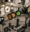
A breakthrough discovery at UC San Diego may help aid the semiconductor industry's quest to squeeze more information on chips to accelerate the performance of electronic devices. So far, the semiconductor industry has been successful in its consistent efforts to reduce feature size on a chip. Smaller features mean denser packing of transistors, which leads to more powerful computers, more memory, and hopefully lower costs. In an effort to help create faster, better and cheaper light sources for chips, UC San Diego researchers, in collaboration with Cymer, Inc., are developing laser-produced light sources for next generation Extreme Ultraviolet Lithography (EUVL).
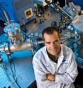
The researchers, led by mechanical and aerospace engineering scientist Mark Tillack, filed a patent in May 2008 for their latest discovery indicating that longer pulse lengths can provide similar performance as short pulse lengths. Tillack and his team found that employing a long pulse in a CO2 laser system used in an EUVL source could make the system significantly more efficient, simpler, and cheaper compared to that using a shorter pulse. Their research findings were recently published in Applied Physics Letters.
Today's semiconductor companies are diligently working on developing EUVL as the leading candidate for next generation lithography tools to produce microchips with features of 32 nanometers or less. While great progress has been made in this field, several challenges still exist to cost effectively field EUVL in high volume manufacturing. Nowadays, the light source in semiconductor lithography is applied directly from a laser through a mask to a wafer. In EUVL, a laser is used to produce extreme ultraviolet light that is sent to a mask and then the wafer.
This indirect process is more inefficient, and could require a very large and very expensive laser source, Tillack said.
"CO2 lasers, which we use in our lab, have two advantages – they are inherently cheaper to build and operate, and they give better conversion efficiency from the laser to EUV light," he said. "Our discovery that long pulses work well enough means that the CO2 laser system can be built and operated more cheaply."
Tillack pointed to possible future applications for EUVL, such as flash memory chips, which will become denser and denser. "Imagine in the future being able to make a 200 gigabyte flash disk memory stick cheaply," he said. "EUVL could make hard disks obsolete".
"We didn't know how to make a powerful source of light in this part of the spectrum before," added Tillack, also an associate director of the UC San Diego Jacobs School of Engineering's Center for Energy Research. "We might be opening new avenues for advanced light sources. We need to continue our research and begin to look at other possible applications."
Source: University of California - San Diego
Other sources
- Researchers Create Enhanced Light Sources For Lithographyfrom PhysorgWed, 9 Jul 2008, 20:49:12 UTC

