Novel quantum dot laser paves the way for lower-cost photonics
With the explosive growth of bandwidth demand in telecommunications networks, experts are continually seeking new ways to transmit increasingly large amounts of data in the quickest and cheapest ways possible. Photonic devices -- which convert light to electricity and vice versa -- offer an energy-efficient alternative to traditional copper network links for information transmission. Unfortunately, these devices are also almost always prohibitively pricey. One way to bring those costs down is to make photonics compatible with the existing silicon microelectronics industry. A promising way to do that is by growing "quantum dot" lasers directly on silicon substrates, according to graduate student Alan Y. Liu of the University of California at Santa Barbara (UCSB) and his colleagues, who include UCSB professors John E. Bowers and Arthur C. Gossard. Although such quantum dot lasers have been grown on silicon before, their performance has not equaled that of quantum dot lasers grown on their native substrates, which are platforms made of similar materials as the quantum dot lasers themselves.
Now Liu and his collaborators in Bowers and Gossard's groups have demonstrated a novel quantum dot laser that not only is grown on silicon but that performs as well as similar lasers grown on their native substrates. The team will discuss its record-breaking results achieved using such lasers at this year's OFC Conference and Exposition, being held March 9-13 in San Francisco, Calif., USA.
The researchers believe the work is an important step towards large-scale photonic integration in an ultra low-cost platform.
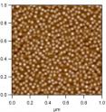
Currently, so-called "quantum well" lasers are used for data transmission. They consist of nanometers-thick layers of light-emitting material, representing the quantum well, sandwiched between other materials that serve to guide both the injected electrical current as well as the output light. A quantum dot laser is similar in design, but the sheets of quantum well materials are replaced with a high density of smaller dots, each a few nanometers high and tens of nanometers across. To put it in perspective, 50 billion of them would fit onto one side of a penny.
"Quantum wells are continuous in two dimensions, so imperfections in one part of the well can affect the entire layer. Quantum dots, however, are independent of each other, and as such they are less sensitive to the crystal imperfections resulting from the growth of laser material on silicon," Liu said.
"Because of this, we can grow these lasers on larger and cheaper silicon substrates. And because of their small size," Liu added, "they require less power to operate than quantum well lasers while outputting more light, so they would enable low-cost silicon photonics."
In their new work, the team grew quantum dots directly on silicon substrates using a technique known as molecular beam epitaxy, or MBE ("epitaxy" refers to the process of growing one crystal on top of another, with the orientation of the top layer determined by that of the bottom).
"The major advantage of epitaxial growth is that it enables us to exploit the existing economies of scale for silicon, which would drive down cost," Liu said. He added that "MBE is the best method for creating high-quality quantum dots that are suitable for use in lasers" and that "the entire laser can be grown continuously in a single run, which minimizes potential contamination."
Source: The Optical Society
Other sources
- Novel quantum dot laser paves the way for lower-cost photonicsfrom Science DailyWed, 5 Mar 2014, 13:31:37 UTC
- Novel quantum dot laser paves the way for lower-cost photonicsfrom PhysorgMon, 3 Mar 2014, 22:31:06 UTC


